An international team of engineers has adapted a medical imaging technique to enable 3D-printed materials to sense where they are being damaged and track how that damage develops in real time
The research, led by academics from the UK and Australia, could unlock new generations of ‘self-sensing’ metamaterials made with intricate lattice structures which are custom-designed to prioritise characteristics such as weight, strength, impact resistance, or flexibility.
These materials could be used in medical implants, aircraft parts or car bodies in the years to come, providing detailed feedback on the condition of the materials as they degrade with age or experience impact-related strain.
The team’s new approach incorporates carbon nanotubes into plastic structures that are architected and 3D-printed with precise arrangements of struts and spaces, giving them a lattice-like structure.
By passing current through the carbon nanotubes via electrodes attached to the materials, the team can use an imaging technique called electrical impedance tomography (EIT) to monitor the material’s structural health as it experiences external loads. The team believes their new research, published as an Early View paper in the journal Advanced Functional Materials, is the first reported use of in situ EIT to monitor damage in 3D-printed architectured metamaterials.
EIT is often used in medical settings to monitor patients’ lung function during hospital stays. It uses electrodes to take continuous measurements of how electricity flows through materials such as human tissues. Analysing these measurements reconstructs images of the material’s interior without invasive procedures, enabling real-time tracking of changes.
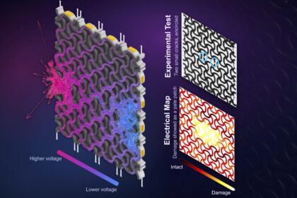
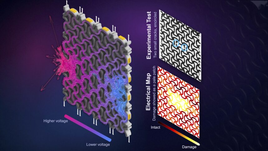
In the team’s research, they used EIT to map changes in electrical conductivity across the structure by passing current and measuring voltage differences through external electrodes attached to structures they designed and printed in the lab as they were stretched to the breaking point. The lattice specimens were rectangular structures measuring 48mm across.
The research expands on previous work from the University of Glasgow’s,Sustainable Multifunctional Materials and Additive Manufacturing (SM2AM) Lab, led by Professor Shanmugam Kumar.
Traditional sensing methods can measure changes in electrical resistance/conductivity at specific points, which suit simple structures but cannot show what is happening throughout complex metamaterials.
In 2024, the SM2AM lab developed a sophisticated modelling framework that could predict how the electrical conductivity of lattice materials changes when they are stretched or compressed. However, the approach is relatively complex, so the team used EIT to monitor conductivity changes across the entire structure rather than only at individual points.
As the materials stretched, the conductive pathways in the lattice changed, altering the way electricity flowed through the structure and the voltages measured at its surface. These changes in electrical behaviour provided information about how the structure was deforming and where damage was developing.
A computer algorithm translated these voltage changes into real-time maps showing how the structure’s electrical properties were changing as damage developed. The system showed where damage was developing and how it was progressing, including damage occurring away from the electrodes used for measurement.
The system also highlighted where damage built up before the lattice broke, providing a possible basis for an early-warning system in future practical applications. The team validated the findings by comparing the system’s results with direct observations of the structures, confirming that it accurately identified where damage developed and where the structures eventually failed.
The algorithm’s maps could localise damage to within about one strut of its actual location. The researchers also pushed the system’s limits by deliberately building tiny cracks into some struts. They found they could track the cracks as they spread outwards under increasing strain.
Professor Kumar, of the James Watt School of Engineering, said, “In this research, we’ve developed a new way to map electrical changes across an entire 3D-printed lattice structure in real time. The output is somewhat like an MRI scan: just as an MRI can show what is happening throughout the body, our approach allows us to see how different parts of the lattice are responding while it is under strain. The engineered lattice architectures enable control over sensing fidelity.
“Conventional measurements can tell us what is happening at a particular location in a material, or provide an overall, averaged indication of the structural health of the whole structure. However, they cannot show us in detail where damage is developing and how it is spreading throughout the structure. Our research shows that, by combining carefully designed lattice structures with EIT, we can obtain this much richer picture of structural behaviour, including detecting damage before the structure ultimately fails.
“This technique could open up potential applications in areas such as structural health monitoring and other advanced engineering systems, although further work is needed to develop and scale the technology for practical applications.”
Akash Deep and Professor Andrew McBride from the University of Glasgow contributed to the research and co-authored the paper, alongside Dr Andrea Samore and Professor Alistair McEwan from the University of Sydney.
The team’s paper, titled ‘Full-Field Damage Monitoring in Architected Lattices Using In situ Electrical Impedance Tomography’, is published in Advanced Functional Materials. The University of Sydney–University of Glasgow Ignition Grants supported the research, and a Vaibhav Fellowship awarded to Professor Kumar by the Indian National Academy of Engineering and India’s Department of Science & Technology also supported it.