
The ability to manipulate material properties with precision is one of the defining challenges of modern materials engineering
From high-efficiency photovoltaics to ultrafast electronics and quantum technologies, researchers are increasingly looking beyond conventional approaches to discover new ways of controlling the behaviour of matter at the atomic scale.
A recent breakthrough by scientists at Argonne National Laboratory has revealed a promising new pathway. By using ultrafast laser pulses to drive coordinated atomic motion in semiconductor materials, researchers have observed a Higgs mode in a semiconductor for the first time – a discovery that could ultimately enable engineers to access entirely new material phases and functionalities.
FOCUSING ON METAL HALIDE PEROVSKITES
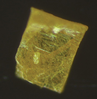
At the heart of the work is a class of materials known as metal halide perovskites. These materials have attracted significant interest because of their highly tunable properties and strong interaction with light, making them attractive candidates for next-generation solar cells, advanced sensors and emerging quantum technologies.
While materials may appear static to the naked eye, their atoms are constantly in motion. Under the right conditions, these movements can become synchronised, creating collective vibrations known as phonons. Understanding how these vibrations influence material behaviour has become a major focus for researchers seeking to engineer new properties on demand.
In the Argonne study, scientists exposed a layered two-dimensional perovskite crystal to ultrafast laser pulses and observed an unexpected response. The light induced a collective vibration that altered the symmetry of the crystal itself.
“When we excite this material, the atoms that make up its structure start to oscillate in more ways than one,” says Richard Schaller, an Argonne scientist and author on the study. “Because of the ways those atomic vibrations are coupled with each other, the collective motion actually changes the material’s structure, driving it toward a state with higher crystal symmetry.”
The significance of the finding extends well beyond a single material system. The researchers discovered that light could steer the crystal toward a structural phase that cannot be reached simply by heating the material. This demonstrates that optical excitation can access regions of the material-property landscape that remain inaccessible through traditional thermal processes.
UNDERSTANDING THE HIGGS MODE
The term Higgs mode may be familiar from particle physics, where the Higgs boson became one of the most celebrated scientific discoveries of recent decades. Similar mathematical concepts, however, appear in a wide range of physical systems.
In materials science, a Higgs mode represents oscillations in the degree of order or symmetry within a system. These oscillations emerge when a material undergoes spontaneous symmetry breaking – a process that causes it to adopt a lower-energy configuration. Perovskite materials naturally exhibit this behaviour.
“You can simulate an ideal perovskite structure, but you won’t find most perovskites in that configuration in nature,” explains Argonne scientist Pierre Darancet, a theorist on the study. “They tend to lower their energy by creating secondary structures that decrease their crystal symmetries.”
What makes the Argonne result particularly noteworthy is that it represents the first observation of a Higgs mode in a semiconductor. Unlike previous observations in superconducting systems and other exotic materials, this discovery occurs in a material platform already considered highly relevant for future electronic and photonic devices.
CHANGING COLOURS
The experiments focused on butylammonium lead iodide, a two-dimensional metal halide perovskite. The material’s bandgap – the energy threshold that determines which wavelengths of light it absorbs – plays a critical role in its electronic and optical behaviour. Rather than generating electrical excitations, the researchers deliberately illuminated the material with light below its bandgap energy.

“In these experiments, when we excite the sample below its bandgap, there’s not enough energy to create electric excitations. Instead, at these very low energies, the light pulse can excite only vibrations,” says Schaller.
As groups of atoms oscillated throughout the crystal structure, the material’s bandgap began changing in real time. Using impulsive stimulated Raman spectroscopy, the team detected rapid periodic shifts in the bandgap that directly reflected changes in crystal symmetry.
“We found that the bandgap increased and decreased periodically and rapidly,” continues Schaller. “Essentially, the colour of the sample oscillated as it rocked through different crystal symmetries – turning redder and then bluer, over and over.”
Theoretical modelling revealed that the light-induced motion combined multiple vibrational modes simultaneously, creating a coherent collective response across the crystal.
“Two frequencies were involved in the bandgap oscillations, and that’s where this material is special. Instead of just one simple vibration, the material displayed a coherent superposition of harmonics, resonating similarly to a violin when you bow its strings,” Darancet adds.
ENGINEERING FUTURE MATERIAL STATES
Different crystal symmetries can produce dramatically different material properties. By controlling symmetry directly with light, researchers could eventually engineer materials whose electrical, optical and structural characteristics can be switched on demand.
“In this study, the oscillations steer the material toward a state with higher symmetry – and with a much lower bandgap – than its ground state,” says Sraddha Agrawal, a postdoctoral researcher at Argonne and theorist on the study. “Our next steps are to try and actually achieve that higher symmetry state, and to explore other light-induced phases in perovskite materials.”
Such control could have far-reaching implications for energy generation, electronics and quantum computing.
“If we can use light to control structural and electronic changes in materials on ultrafast timescales – for example, switching a material between conducting and insulating states every picosecond – they might find use as optical switches in modern microelectronics and quantum technologies,” adds Argonne postdoctoral researcher and experimentalist Ayushi Shukla. “Also, stabilising novel, high-symmetry phases with low bandgaps could open exciting opportunities for photovoltaic applications.”
The study ‘A meta stable tetragonal phase in two-dimensional halide perovskite lattices driven by a coherent Higgs mode’ is published in Nature Materials