
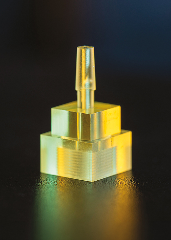
Jake Collins explains to Louise Davis how micro-precision 3D printing solutions are offering electronics design engineers game-changing levels of freedom.
One of the things Jake Collins finds particularly satisfying about his work is its lack of constraints. Collins is senior applications engineer at Boston Micro Fabrication, a US-headquartered manufacturer of micro-precision 3D printers.
He describes the freedom that micro-precision 3D printing brings enthusiastically. “When you look at conventional manufacturing processes, they have built-in ‘rules’ that engineers and designers have learned to work within and those constraints on the process dictate how a part can be designed,” Collins begins.
“Consider design limitations on mould cavities and CNC machining as examples. Both of these processes are great manufacturing techniques for many products currently out in the world but they may limit an engineer on how they can design a part – whether it’s avoiding internal overhangs that can’t be moulded or machined, or wall thicknesses below a certain size due to tool sizes,” he adds.
Collins points to a 3D printing technique called projection micro stereolithography (PµSL) as the way to remove many of those sort of constraints. “It builds parts voxel [volumetric pixel] by voxel and layer by layer, allowing for extremely high dimensional control as well as no restrictions from conventional processes, such as a mould-pull direction or directional paths of cutting tools,” he explains.
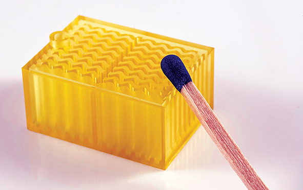
“What this gives us is true control over 3D routing of channels and interconnects in electronic components, as opposed to planar or layered routing from limitations in manufacturing. It also allows for geometry that would be unmanufacturable previously – such as a latticed section within a part – that mould tools and conventional machining would not be able to do. PuSL enables engineers and designers to design for function, not around the manufacturing processes that constrain the design traditionally,” Collins emphasises.
GRAND DESIGNS
Removing longstanding design constraints is an important part of helping designers to meet the challenges associated with today’s trend for electronic devices becoming ever smaller and more complex.
On this, Collins observes: “Because of its design freedoms, additive manufacturing allows for a shift in thought processes from assembly-based design to a performance-based design. Traditionally, all components would be manufactured separately (using separate processes due to constraints on the manufacturing process) and then assembled into the final part. This introduced additional labour, tolerance stack-ups and more failure risk. Now with micro-additive manufacturing, part consolidation is possible and end parts can be designed as a single structure that combines many of these aspects.”
The engineer notes that although this process may not replace every single component in every material, as some perform specialised tasks, consolidating a number of components can help to maximise performance and minimise risk of failure through multiple modes. “For example, looking at fibre arrays since they are a high-priority type of part with data centres, a printed fibre array guide could introduce a very close-packed spacing between fibres at very high tolerance, while also allowing for internal direction change and tapering the bore geometry and size,” Collins details.
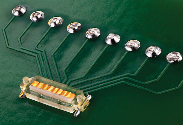
“This can provide lower signal loss and allow directional changes that would be impossible with traditional methods. Being able to pack more fibres into a space and route more efficiently could allow for higher performance and smaller end parts.” He adds: “Other examples of parts we have already seen include embedded fluid channels for thermal management, as well as creating vertical interconnect accesses (VIAs) through selective metallisation, which would require a much more complex approach or even be impossible to manufacture via other methods.”
ARCHITECTURAL DIGEST
Rather than only making things smaller, Collins believes that micro-precision 3D printing could also enable electronics designers to rethink traditional architectures entirely: “As we have advanced further we have definitely become more complex and pushed towards miniaturisation of devices and components across many industries. Miniaturising existing architectures relies on the same thought process of designing around limitations that may have been present when creating the existing design. Micro-additive asks a different question: if you weren’t constrained by existing manufacturing methods (i.e. planar PCBs, discrete connectors, etc.) what would you actually design?’”
Expanding on this, he says: “Looking at it from that point of view allows engineers to approach the problem they are trying to solve in a different way. Some ideas we think could be interesting in the future include designing based on 3D electronics, not a stack-up of 2D boards. Using interconnects that run through the extents of the part in X, Y and Z without limitations allows for more natural routing; think vasculature of blood vessels instead of rigid 2D stacks.”
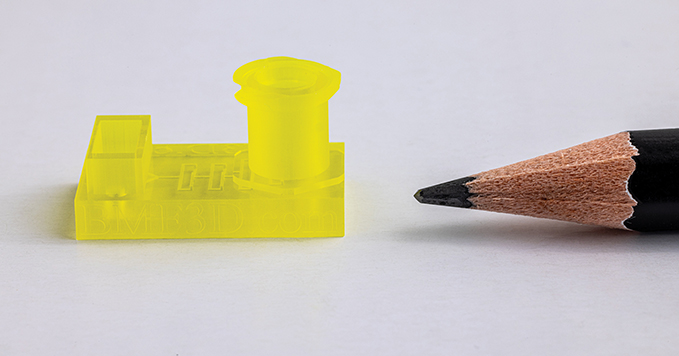
Collins cites the use of specific connectors and interposers for an exact application as another example here – essentially custom parts per design instead of using the more standardised designs that are often used today purely because they’re more readily available. “As you push into the smaller sizes of parts, such as sub-mm fibre and sensor arrays, there aren’t as many off-the-shelf parts available and creating custom designs allows for capture of those incremental performance gains,” he explains.
AREAS OF INTEREST
When asked which areas of electronics design he thinks could be most fundamentally transformed by micro-precision 3D printing, Collins uses lessons learned from current successes to inform his future predictions, “A few of the different sectors that can be transformed by micro-additive are ones that already have been, to some extent,” he observes.
Photonics and interconnects are top of this list. Colins says: “Fibre alignment, coupling and packaging require exacting tolerances and smaller and smaller features, which lend themselves extremely well to micro-additive. Building on that, complex 3D channel geometry – such as tapered/bored, internal routing changes and HCP arrays – all of which micro-additive is uniquely good at, are giving higher performance and expanding that industry further.”
The expert cites radiofrequency (RF) and microwave components as another key area. “This has been a space we’ve been involved in for a while because micro-additive allows for 3D antenna and waveguide geometries that just wouldn’t be possible with traditional manufacturing, and these new parts are designed to outperform the planar geometries. Our customers can quickly produce end-use parts that outperform traditional planar parts.”
As well as those industrial applications, Collins highlights consumer micro-devices as a significant application area – particularly hearing aids, smart glasses and wearable sensors. “All of these are designed to be minimally invasive and blend in seamlessly with the wearer, so creating smaller, more precise versions has been a big goal in the industry,” he says.
FREE TO CHOOSE
Regardless of the type of application, Collins says that the overall message he’d like to share is that micro-additive manufacturing isn’t just about ‘printing small stuff faster’. Rather, he notes, “It’s that it enables design freedom and delivers complexity for free for designers, so their focus can be on the application and performance, rather than the constraints of manufacturing.”
“It also allows for faster and cheaper design cycles, giving engineers more time and flexibility to test new designs without the fear of failure from time and cost in traditional methods. As devices and electronics get smaller and require higher performance, micro-additive manufacturing can change the rules and open new ways to tackle these challenges,” Collins adds.

CASE IN POINT
One real-world example of the design freedom micro-precision 3D printing delivers can be found in the work of one of BMF’s customers, Horizon Microtechnologies, which specialises in RF solutions. “We worked with their team on some corrugated horn antennas for millimetre-wave systems. These are a pretty typical type of design, but the internal geometries (the corrugations) that give it high performance are typically hard to manufacture,” explains Collins.
“As you move into higher frequencies, there is an inverse relationship with feature size, and the features become smaller and require higher tolerances. With the scale required for high-frequency applications, typically a few hundred microns, traditional machining runs into limits and requires multiple parts to even produce, which adds the possibility of alignment error. Using the micro-additive manufacturing approach, the entire horn geometry was produced as a single part,” he details.
From there, Horizon applied its proprietary conformal metallisation process directly to the printed part, which allowed for full metallisation through the corrugated grooves at extremely high precision. Collins comments: “This hybrid approach resulted in shorter lead times, more freedom of design (so potentially higher performance) and minimised RF losses, as the part has minimal surface roughness and no parts to assemble and introduce alignment error. This shows that micro-additive isn’t just a prototyping option; companies are already using it to produce high-performance end-use parts while avoiding the constraints of traditional manufacturing.”
Read the October issue of International Design Engineer magazine here, or visit our magazine archive for all our recent publications.