
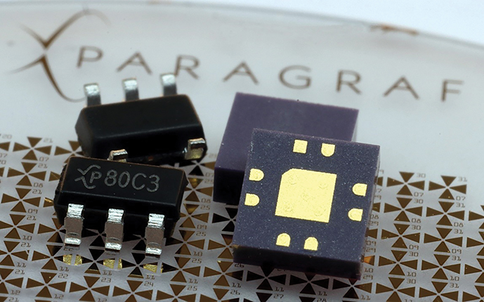
How Paragraf are unlocking graphene’s potential with their scalable, electronic grade graphene for a wide-range of industries, including electric vehicles
Andrew MacInnes, chief development officer at Paragraf, shares the company’s latest technical breakthrough in electronics manufacturing
More than 20 years after the groundbreaking discovery of graphene by Andre Geim and Konstantin Novoselov at the University of Manchester, the “wonder material” continues to hold vast potential across multiple industries. Yet, despite early optimism, especially in electronics, graphene’s commercial adoption has lagged behind the initial hype.
In a recent technical talk at The Advanced Materials Show, Andrew MacInnes, chief development officer at Paragraf, a UK-based company headquartered near Cambridge, sought to reframe this narrative and demonstrate how Paragraf’s innovations in scalable, electronics-grade graphene production are now unlocking the material’s long-promised potential across a wide range of industries, including electric vehicles (EVs).
“We don’t make metric tons of graphene,” he said. “We’re not chasing bulk composites. We’re addressing the electronics sector and solving the engineering problem of how to deploy graphene at scale with precision.”
UNDERSTANDING GRAPHENE
To contextualise the discussion, MacInnes provided a brief overview of graphene’s structure. Graphene is a single atomic layer of carbon atoms arranged in a hexagonal lattice, peeled from graphite. It possesses superior properties: optically transparent, chemically inert, stronger than diamond, and most notably, highly conductive.
“Graphene is derived from graphite. It’s the only thermodynamically stable element in the sp2 hybridised form,” MacInnes explained. “Take a single layer of graphite, and you get a material more strongly bonded than diamond, with unmatched electrical and mechanical properties.”
These exceptional properties stem from graphene’s unique band structure. First theorised by P R Wallace in 1947 while studying nuclear reactions, the linear dispersion relationship between energy and momentum – where the valence and conduction bands meet at a Dirac point – predicted extraordinary carrier mobility.
“Electrons in graphene behave more like waves than particles. They move at velocities approaching those of photons; an order of magnitude beyond any other semiconductor,” MacInnes said.
BRIDGING SCIENCE AND ENGINEERING
Theoretical perfection, however, does not guarantee practical application. Real-world deployment introduces unavoidable imperfections. Graphene must be placed onto a substrate and encapsulated for device integration. At every stage – exposure to air, contact with polymers, or transfer between materials – its properties degrade.
“The race isn’t just about making graphene,” MacInnes emphasised. “It’s about preserving its integrity through scalable engineering processes.”
Traditional methods like chemical vapour deposition (CVD) on copper foils followed by transfer to silicon introduce contamination, wrinkles, and defects. Other methods such as exfoliation or reduction of graphene oxide lack the reproducibility and quality required for electronic devices.
This is where Paragraf’s approach distinguishes itself. Rather than transferring graphene, the company grows single-layer graphene directly on electronic-grade substrates such as sapphire or silicon carbide using proprietary plasma-enhanced CVD techniques.
“We grow directly onto the end-use substrate. No transfer, no gaps, no multilayers – just a continuous, defect-minimised graphene film ready for device fabrication,” MacInnes explained. “This is what allows us to deliver electronic-grade graphene at commercial scale.”
FROM MATERIAL TO PRODUCT
With robust control over material quality, Paragraf has focused on two core product categories: Hall effect sensors and graphene-based field effect transistors (GFETs) for molecular sensing.
Hall sensors benefit from graphene’s high carrier mobility, which allows for ultra-low-power operation and high sensitivity across a range of applications, from electric vehicles to cryogenic sensing in quantum computing.
“We’re already shipping sensors into markets that require precise, low-noise magnetic field detection at temperatures approaching absolute zero,” MacInnes said. “That’s only possible because graphene remains functional in such extreme conditions.”
GFETs, on the other hand, use the ambient environment – gas, fluid, or solid – as the gate input, making them ideal for biosensing and molecular diagnostics. Paragraf is developing sensors capable of detecting biomarkers in breath, such as acetone for diabetic ketoacidosis, or in liquid samples for early-stage medical diagnostics.
“These devices operate at incredibly high transconductance. A small change in molecular charge on the surface translates to a significant electrical response. That’s what gives us single-molecule sensitivity,” said MacInnes.
EV APPLICATIONS
In addition to quantum computing and medical diagnostics, Paragraf’s graphene-based Hall effect sensors are proving highly applicable to battery management systems (BMS) in EVs. Precise current sensing is critical for monitoring charge and discharge cycles, detecting cell imbalances, and ensuring thermal and electrical safety. Graphene’s ultra-high electron mobility enables low-noise, high-resolution measurements at extremely low power levels, making it ideal for continuous monitoring in energy-sensitive environments.
“With graphene, we can detect subtle current excursions that signal early battery degradation or potential failure,” said MacInnes. “This supports predictive maintenance strategies and extends battery life, which is essential for improving EV performance and reducing operational costs.”
Furthermore, the sensors maintain stability across a wide temperature range, a key requirement in EV applications where systems operate from sub-zero climates to intense summer heat.
ENGINEERING MATURITY
Beyond its producing capabilities, Paragraf is positioning itself as a foundry partner for the wider industry. It has implemented standard semiconductor quality control and statistical process control to bridge the gap between lab-scale innovation and industrial production.
“This is no longer just scientific exploration. It’s now an engineering discipline,” MacInnes said. “We’ve moved from intuition-driven discovery to statistically reproducible device fabrication on wafer-scale platforms.”
The company recently transitioned into a new purpose-built facility in Huntingdon to support wafer-scale manufacturing and meet the volume demands of customers in automotive, aerospace, quantum computing, and medical diagnostics.
“We don’t intend to be the end-product supplier forever,” said MacInnes. “Our goal is to enable our partners – OEMs, fabs, and device companies – to incorporate 2D materials into their own systems. We are building a graphene foundry for the electronics industry.”